Let the sun power your day
Enhancing PV technology affordability, supply security, and sustainability is key to achieving a clean energy transition and zero-emissions goal.
Let’s build a green world together.



Next-Generation Photovoltaics
Tin-Halide Perovskite
Thin Films
Tin halide perovskite solar cells show promising potential with high power conversion efficiencies and low-cost fabrication processes, though ongoing research targets further improvements in stability and scalability for broader commercial viability.
Performance
Characteristics


partners
>
researchers
>
technologies
>
publications
bn. €
Our Mission
Catalyzing the Future of Solar Energy
Our mission is to address the critical challenges facing the photovoltaic sector through groundbreaking research and development. By advancing thin-film PV technology and strengthening the European PV value chain, we aim to empower communities and industries with reliable, cost-effective, and sustainable solar energy solutions, fostering a cleaner and more resilient energy future.
<35
€/sqm.
We aim to cut solar power costs by over 50% with advanced perovskite technology and efficient production.
>25%
PCE
We enhance solar cell durability and versatility, boosting energy output in compact spaces, crucial for urban settings.
>2000
hours
We enhance perovskite cell stability with new compositions and encapsulations, extending lifespan and commercial viability.
Key Goals
Perovskite solar technology holds great promise for the future of solar energy.
Our cutting-edge research in thin-film PV technology is poised to break through current barriers.

Increase Power Conversion Efficiency

Optimize Device Architecture

Module Fabrication
Our Technology
Morphology
Plasma
Device
MorphoColor
Assembling
Testing
Installation
Smart Home
Morphology
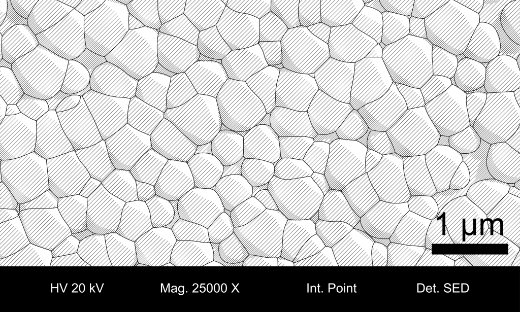
The morphology of tin-based perovskite in scanning electron microscopy (SEM) reveals a multifaceted structure with well-defined crystal facets and surface features. SEM images provide insights into the size and shape variations of perovskite crystals, crucial for their electronic and optical properties.
Our Technology
Morphology
Plasma
Device
MorphoColor
Assembling
Testing
Installation
Smart Home

Morphology
The morphology of tin-based perovskite in scanning electron microscopy (SEM) reveals a multifaceted structure with well-defined crystal facets and surface features. SEM images provide insights into the size and shape variations of perovskite crystals, crucial for their electronic and optical properties.
Learn more
Our Technology
Morphology
The morphology of tin-based perovskite in scanning electron microscopy (SEM) reveals a multifaceted structure with well-defined crystal facets and surface features. SEM images provide insights into the size and shape variations of perovskite crystals, crucial for their electronic and optical properties.
Life cycle and circularity
Showcase a threefold reduction in raw material supply risk and a substantial increase in material recyclability compared to existing thin film PV technologies on the market.
Our way
Harnessing prosuming’s dynamic energy, we explore the boundless potential of PV foil—lightweight, flexible, and available in any color. Our pioneering plasma-assisted techniques refine tin perovskite technology, enhancing reproducibility and grain sizes for sustainable solar solutions.

Lead-free

Plasma

Flexible

Light weight

Any color

Prosuming
Consortium


Temicon
Temicon is a worldwide series producer of nano and micro structured films for innovative displays, LED, Solar or Optics applications. The company temicon is a pioneer in lithographic production of micro- and nanostructures on large, seamless surfaces and replication by roll-to-roll or roll-to-plate nanoimprint processing and electroforming.
Workpackes


Latest news
Pioneer, innovator or industrial giant?
Forging ahead with the commercialization of our transformative technologies, we’ve established strategic collaborations with renowned industry leaders who share our vision for the future of solar energy.
Let’s drive innovation, transform markets, and lead the way towards a sustainable energy future together.
Early
Adopters


External Expert Advisory Board

Philipp Semmler
CEO, Blue Minds Company

Frank Hermanns
CEO, Smart Building Innovation Foundation

Laura Holzer
Sustainability Manager, ASFINAG


